DIONICS, INC.
Phone: (516) 997-7474
65 Rushmore Street Fax: (516) 997-7479
Westbury, NY 11590 Website:
www.dionics-usa.com
DIG-11-8-30-DD; DIG-12-08-30-DD; DIG-22-8-30-DD
Photovoltaic MOSFET Drivers With Dynamic Discharge*
*US Patent 4,931,656
Features:
ÿ
Fast Turn Off, Active Gate Discharge
ÿ
Dielectrically Isolated
ÿ
Logic Circuit Compatibility
ÿ
High Open Circuit Voltage
ÿ
High Operating Temperature
ÿ
Fast Response Time
ÿ
High Isolation Resistance
ÿ
Excellent Input/Output Linearity
ÿ
Self Limiting Gate Voltage
Applications:
ÿ
Gate Drive For MOS devices
ÿ
Gate Drive For SCR
ÿ
Solid-State Relays
ÿ
Interface Between Logic Circuits & External Loads
ÿ
A.T.E. (Automatic Test Equipment)
ÿ
Switching Equipment
ÿ
Isolation Amplifiers
ÿ
Load Control From Microprocessor I/O Ports
ÿ
Thermocouple Open Detectors
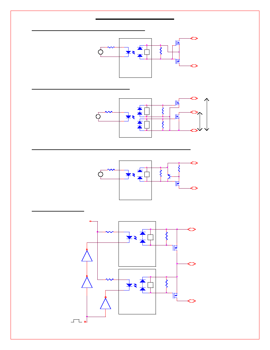
Description:
The photovoltaic MOSFET-driver is a State-of- the-Art, optically coupled floating power source used primarily to control
MOSFETs or IGBTs when electrical isolation between input and output is required.
In addition to the infrared LED and photovoltaic (PV) diode array, each of the DD (Dynamic Discharge) products
contains circuitry that rapidly discharges the power MOSFET gate when the LED is deactivated. The unique rapid
discharge features of the photovoltaic MOSFET-drivers make them particularly useful for high-side switching of N-
channel MOSFETs in solid-state relays, DC motor control and switching regulator applications.
The typical input circuit to the LED is a limiting resistor connected in series with the LED. When activated, the LED
emits infrared light towards the photovoltaic diode array, which then responds by generating an open circuit voltage (V
oc
),
thus disabling the turn-off circuitry. The self-limiting photovoltaic output of the diode array is floating and therefore, can
be safely applied directly to the gate and source of a MOSFET, regardless of the source potential of the MOSFET. When
the LED is deactivated, the active turn-off circuit discharges the capacitive input of the MOSFET. The active turn-off
circuitry is designed such that the turn-off time of the MOSFET is relatively independent of the input capacitance of the
MOSFET over a range of 50 to 5000 pF. Standard packages include low cost plastic mini-dips and hermetic 8-pin DIP
ceramic side brazed.
v
Package Layout:
0.025
0.020
0.250
DIG-11
8-30-DD
xxxx
0.070
0.380
0.185
0.185
0.250
0.025
0.070
0.380
0.020
DIG-12
8-30-DD
xxxx
Pin Designation
Pin
Part Number
Number
11-8-30-DD 12-8-30-DD 22-8-30-DD
1
Input +
Input +
Input 1+
2
Input -
Input -
Input 1-
3
Not Connected Not Connected
Input 2+
4
Not Connected Not Connected
Input 2-
5
Not Connected Output1+
Output2+
6
Output +
Output1-
Output2-
7
Not Connected Output2+
Output1+
8
Output -
Output2-
Output1-
07/2002

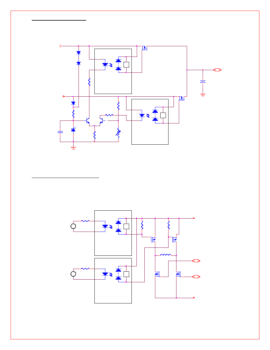
DIG-11-8-30-DD; DIG-12-8-30-DD; DIG-22-8-30-DD Equivalent Circuits:
LED
PV
T.O
Cir.
3
2
1
7
6
8
1
5
6
8
7
4
T.O
Cir.
3
2
LED
PV
T.O
Cir.
PV
3
1
8
5
6
LED
PV
T.O
Cir.
T.O
Cir.
2
7
LED
PV
4
DIG-11-8-30-DD
DIG-12-8-30-DD
DIG-22-8-30-DD
Ceramic Package Only
v
Individual Channel Electrical Characteristics (T
a
=25
0
C)
Model Number
DIG-
11-8-30-DD; 12-8-30-DD; 22-8-30-DD
Unit
Parameter & Test Condition
Symbol
Min.
Typ.
Max.
Open Circuit Voltage*
V
oc
I
led
= 2mA
8.5
9.5
-
V
I
led
= 10mA
9.5
10.5
-
V
I
led
= 30 mA; 50% Duty Cycle
10.5
11.5
-
V
Short Circuit Current
I
sc
I
led
= 2mA
1.0
3.0
-
Ï A
I
led
= 10mA
10.0
15.0
-
Ï A
I
led
= 30 mA; 50% Duty Cycle
30.0
50.0
-
Ï A
LED Forward Voltage
V
r
I
f
= 20mA
DIG-11-8-30-DD
-
1.3
1.7
V
DIG-12-8-30-DD
-
2.6
3.4
V
DIG-22-8-30-DD
-
1.3
1.7
V
LED Reverse Current
I
r
V
r
= 5V
0.1
10.0
Ï A
Off State Voltage
V
off
I
off
= 10
µ
A; I
led
= 0mA
-
0.65
1.0
V
Isolation Voltage
V
iso
2500
-
-
VDC
Temperature Coefficients
Ë V
-
45
-
mV /
0
C
I
led
= 10mA
Ë I
-
0.5
-
%I /
0
C
Turn-On Time
I
led
= 30 mA
T
on
-
100
-
Ïs
C = 1500pF; Voc to 10%
Turn-Off Time**
I
led
= 30 mA
T
off
-
3.0
6.0
Ïs
C = 1500pF; Voc to 50%
* Ceramic version differs. Contact factory for specifications
** For proper turn -off operation, gate must be charged to 90% of its final value before turn -off initiated
v
Absolute Maximum Ratings (T
a
= 25
0
C)
LED Forward Current
LED Forward Current
LED Reverse Voltage
Output Discharge Current
Operating Temperature Range
Operating Temperature Range
Storage Temperature
Power Dissipation
Steady State
Peak 10% Duty Cycle
Plastic D.I.P
Side Braze D.I.P
100 mA
250 mA
10V
50mA
-40 to 85
0
C
-50 to 125
0
C
-50 to 125
0
C
250 mW